
Many people have heard of Moore’s Law, that the number of transistors that can be put on a chip doubles every two years. Gordon Moore, a co-founder of Intel, noticed this in 1965, and it’s held true pretty much ever since. It has led to the fantastic improvement in the performance and cost of semiconductors, and has changed the world. I actually got to hear Moore give the keynote speech at a conference a few years ago, and he got a standing ovation! I have never seen that at any other technical talk.
Yet unless you’re in the chip game, you have almost certainly not heard of Robert Dennard. He’s the one who laid out just to accomplish that doubling, how to maintain that incredible rate of growth without having the chips melt. In a paper in 1974, Design of Ion-implanted MOSFET’s with very small physical dimensions, he and five other authors from IBM proposed what has since been called Dennard Scaling. After Moore’s paper itself, this is probably the most important paper ever published about chips.
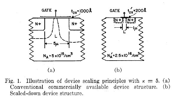
The above figure is taken from his paper. It shows how to go from a transistor with a gate length of 5 um down to one with a gate length of 1 um, a scaling of 5. The gate length is the distance from one terminal of the transistor to the other, and the smaller it is, the less time it takes to switch. Yet at the same time that the gate length is shrunk, the oxide that separates the gate terminal from the silicon must also be thinned or else the channel will not turn on. The density of doping in the two side terminals must also be increased, or else the junctions will overlap and again the transistor won’t work. In addition to all that, the voltage on the gate must be reduced or else the transistor will draw too much power. All of these constituted Dennard’s scaling rules, and they worked for the next 40 years.
Yet this wasn’t Dennard’s only big contribution. In 1967, when he was 35, he filed a patent (US3387286A) on the one-transistor-one-capacitor memory cell, a circuit that has since become known as Dynamic Random Access Memory, or DRAM. You’re using some right now as you’re reading this. It’s the answer to one of the primary problems in computers – how to store the data that the machine deals with in a way that is fast and cheap:

It consists of an array of tiny little capacitors, each of which can store a charge that can represent a one or a zero. One end of the capacitor is tied to a transistor, which can connect it to a “bit line” to be read or written. The gate control of the transistor is tied to a “word line” which turns it on, and enables a whole column of bits to be accessed at once. The transistors and capacitors can be arrayed as dense arrays called mats, and a lot of mats can be fitted on a chip. Current chips can fit 300 million bits onto one mm2 of silicon. That could hold about 40 novels on a dot the size of this: o.
The brilliant insight here was that the charges don’t have to be permanently stored. They tend to leak away over time, but the circuitry can refresh it every so often by doing a read and then a write back of the same data. That’s why this is called dynamic RAM. There’s another method called static RAM (SRAM) which does not need refreshing, but is nowhere near as dense. Here he is with one of the early DRAM chips, and with unfortunate 70s hair and tie:

DRAM is one of the five core circuits of all of semiconductors. The others are the 6-transistor SRAM, the CMOS static combinatorial gate, the differential sense amp, and the NAND flash memory cell. They account for practically all of the transistors ever made, even now.
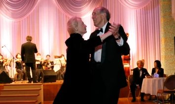
Dennard is still around at age 91. He joined IBM in 1958 at age 26 after getting a PhD from CMU, and spent his entire career there. He holds about 80 US patents, with the latest (US9666267B2) filed in 2016. It describes a way to adjust a transistor threshold voltage by means of a buried device, an interesting and important technique. His first was in 1959, at age 23, and his peak patent creativity was from 2010-2013 when he was age 78 to 81. He had a patent dry spell from 1980 to 2000, when he was probably in management. He also worked on word-line and bit-line redundancy, and on eliminating latchup, a serious problem in early CMOS chips. He has won every award imaginable in the field, as one might expect. Here he is dancing with his wife Jane at the Imperial Palace in Tokyo after winning the Kyoto Prize in 2013:
Now there’s a life! He still loves to dance and to play in local musical groups.
So where did all this talent come from? Part of it was from the support of IBM, which has been a semiconductor leader from the beginning. They didn’t invent integrated circuits, but have made huge contributions to the field. They still do, even though they can’t afford their own fabs any more.
Yet Dennard’s own background must have helped. He grew up in a poor family of farmers in East Texas in the Depression-era 1930s. He went to a one-room schoolhouse for grades 1 to 3. He was the youngest of four children, and his three older sisters went off to work during WW II. They left their libraries, so he grew up reading H. G. Wells and Mark Twain. He was too small for sports in high school, but he had musical talent and joined the school band playing French horn. When it came time for college, all his parents could afford was the local junior college, but then Southern Methodist University offered him a band scholarship. That exposed him to the wider world, and he took off from there.
In 2014 he talked about his own process:
I often wake up in the middle of the night with a solution to a problem that I have been working on previously. Many inventors have described similar experiences to me, including getting out of bed to make notes or drawings before going back to sleep. Others have described significant inventions made while driving, which apparently leaves a lot of the mind free, at least before cell phones. My invention of the DRAM memory cell came early one evening after I came home stimulated and challenged from listening to a talk about a competing research project. The basic idea came in a moment, but there were a couple of months of perfecting it before the final simplification to a single transistor came in another flash of inspiration. At a National Inventors Hall of Fame event, while I was talking with four other inductees, I discovered that all five of us were raised in rural areas or small towns, and most started their education in one-room schoolhouses. We all were left on our own a lot with plenty of free time to develop our ideas about life. Now that may not be the key to our subsequent successes, but it surely is a counter argument to many of the things that are considered necessary for the younger generation today. I developed a very slow thinking process in my early days, and I believe that is why I am able to bring great concentration to a problem and engage my whole brain in finding a creative solution.
You might think that a tough childhood in a remote area would leave a person uncurious and ignorant, but not if they have a stable family and good access to books. The lack of distraction gave him unusual powers of concentration. Then he got into a field with massive opportunities for people who could think deeply about the subject, and away he went. Semiconductors have been so worked over in the last 70 years that those opportunities are probably no longer there, but the world is full of new challenges for young people with the same ability to focus. Find an institution that supports intense work, and dig in!
